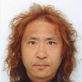

Masami Hane


Keio University

Tell me more about Masami Hane?
Masami Hane is a highly experienced professional with 36.6 years of work experience. He has a strong background in advanced TCAD technology development, particularly in process/device simulation model research and development. He has worked at prestigious institutions such as Keio University and NEC Corporation, where he held various positions including Department Manager and Associated Manager. Masami Hane has also contributed to the development of 45nm-32nm CMOS platform devices. He has a Ph.D. dissertation and has been actively involved in the early development of 45nm-32nm CMOS platform devices.
For inquiries about Phone Number and Email, please click here Unlock Contact
Emails and Phone Numbers
About
1987: Graduated Keio University, Master of Science and Technologies.1987-1993: Engaged in advanced TCAD technology development, especially process/device simulation model research and development in NEC Corporation. Microelectronics Research Laboratories.1993-1994: Visiting Scholoar in Center for Integrated Systems, Stanford University. engaged in Etching/Deposition process simulation modeling project "SPEEDIE" of Prof. K. Saraswat. 1994-1997: Associated Manager of advanced TCAD process/device modeling group, in Silicon System Devices Research Laboratory, NEC Corporation.1996-1999: SELETE 3D Process/Device Simulation tool developemnet project. 1997-2007: Manager of advanced CMOS device research group, in Silicon System Devices Research Laboratory, NEC Corporation. Engaged in early development of 45nm-32nm CMOS platform devices. 2003: Ph.D. dissertation approved by Keio University, in Electrical Engineering.2008-2011: In IBM preT0 CMOS device research project, as an project manager of Renesas Elecronics America, working in Albany, NY. Engaged in 20nm-14nm bulk CMOS devices early development. 2011-2013t: Department head, LSI device research laboratory, Renesas Electronics Corporation.----------------- International Conference Activity --------------1998-present : IEEE Electron Devices Society, AdCom of TCAD Program Chair of 2005 SISPAD (International conference of Simulation of Semiconductor Processes and Devices The conference is the leading forum for Technology Computer-Aided Design (TCAD) 2001-2002 IEDM (International Electron Devices Meeting) program committee of Modeling/Simulation 2006-2007 IEDM program commitee of Modeling/Simulation2007 SSDM Area3 Chair 2008-2009 IEDM Asian arrangement chair2010 IEDM Publication Chair2012-2013 VLSI symposium, Technology Short Course Organizers/Chairs
...See MoreWork Experience
Department Manager
Semiconductor Manufacturing
Masami Hane's Professional Milestones
- Department Manager (1987-04-01~): Streamlining operations and optimizing team effectiveness through effective communication and collaboration.
Education

電気工学科
1981-1987Certification
Colleagues

Charles A. Kawashima
Vice President | Chief Executive Officer
Jason Chiang
Chief Executive Officer | Founder

Fujiko Yamaguchi Hohl
Chief Of Staff | Chief Executive Officer | Vice President Of Sustainability Promotion Office

Hidetoshi Shibata
Chief Executive Officer

Hisao Sakuta
Chief Executive Officer
Other Named Masami Hane
Frequently asked questions
We found 1 Masami Hane's email addresses
We found 1 Masami Hane's phone numbers
Masami Hane works for Renesas Electronics
Masami Hane's role in Renesas Electronics is Department Manager
Masami Hane works in the industry of Semiconductor Manufacturing
Masami Hane's colleagues are Charles A. Kawashima,Jason Chiang,Fujiko Yamaguchi Hohl
Masami Hane's latest job experience is Department Manager at Renesas Electronics
Masami Hane's latest education in Keio University


