 Staff Failure Analysis R&D Engineer / Pathfinding / Materials Scientist / Electron Microscopy at Intel Corporation@ Intel Corporation
 Beaverton, Oregon, United States
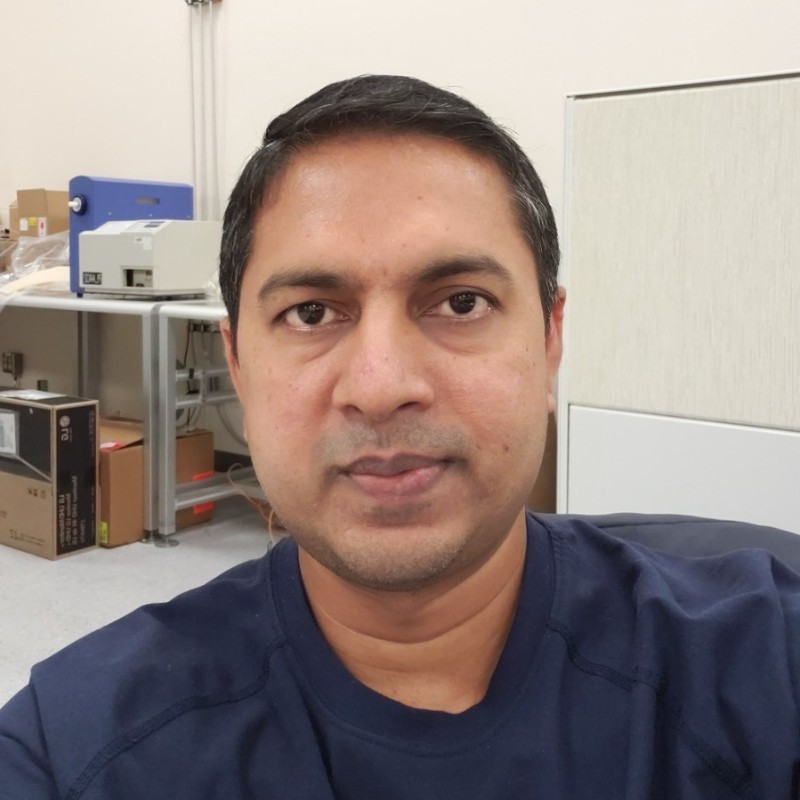
Prakash Palanisamy, PhD
 GET FULL PROFILE
Government College of Engineering, Salem
 Real-Time AI Research
Tell me more about Prakash Palanisamy, PhD?
Prakash Palanisamy, PhD is an experienced Materials Scientist with 19.2 years of work experience. He has a strong background in metals, semiconductors, ceramics, intermetallics, and magnetic materials. Prakash is skilled in materials characterization, imaging, chemical and structural characterization, and failure analysis. He has expertise in metallurgical processes and mechanical testing of materials. Prakash has worked at Intel Corporation as a Failure Analysis R&D Tem Engineer-q&r and has contributed significantly to advanced materials development for components research and pathfinding. He is based in the United States.
For inquiries about Phone Number and Email, please click here Unlock Contact


Emails and Phone Numbers
About
• Experienced Materials Scientist with strong fundamentals and working experience in metals, semiconductors, ceramics, intermetallics, magnetic materials, metallic glasses. • Excellent understanding of structure-processing-property correlation of Advanced Materials. • Proficient in materials characterization. Expert in imaging, chemical and structural characterization using TEM/STEM/EELS, DIB, SEM, XRD, DSC, TGA/DTA, SIMS analysis. • Strong knowledge in metallurgical processes and mechanical testing of materials. • Failure Analysis Expert. Defect investigation using SEM/TEM/Tomography. • Experience in Grain orientation analysis. Grain size-mechanical/electrical property correlation. • Performed channel strain analysis using Nano-beam e-diffraction, Electron-Energy loss spectroscopy, Precession e-diffraction, In-situ electrical biasing in TEM for electro-migration, In-situ heating and cooling to study phase transformation, STEM tomography, HR-TEM of SiGe, GaN, GaAs. • Fabricated small structures and TEM sample preparation using SEM-FIB/DIB. • Lean six-sigma green belt, proficient in design of experiments (DoE), statistical process control and utilization of statistic tools such as JMP. • Strong knowledge and experience with semiconductor device physics and manufacturing process such as thin film deposition using ALD, CVD, PVD and etch cleans, lithography, Metallization and semiconductor device testing. Proficient in Front-End, Back-End of Line process, Novel Interconnect Materials. • Good teamwork and analytical capability; collaborated across multiple teams in Intel corp. Guided and contributed significantly for advanced materials development for components research and pathfinding.
...See MoreWork Experience
Staff Failure Analysis R&D Engineer / Pathfinding / Materials Scientist / Electron Microscopy at Intel Corporation
Failure Analysis Research And Development - Quality & Research
Semiconductor Manufacturing
Prakash Palanisamy, PhD's Professional Milestones
- Graudate Research Assistant (phd) (2008-04-01~2011-03-01): Research collaboration and strategic decision-making to advance research at the field of medicine.
- Failure Analysis Research And Development - Quality & Research (2012-03-01~2017-06-01): Designed and implemented and evaluated data models to optimize testing process and drive continuous improvement.
Education
Metallurgical Engineering
915148800-1009843200Skill
Tem
Fib
Xrd
Sem
Spectroscopy
Characterization
Materials Science
Scanning Electron Microscopy
Metallurgy
Nanotechnology
Powder X Ray Diffraction
Materials
X Ray
Mechanical Testing
Experimentation
Design Of Experiments
Sputtering
Certification
Colleagues

Michael Groiser
Senior RF & Failure Analysis Engineer | Senior CAD Navigation App Engineer | Owner

Prajwal Talanki
Product Owner
Nitasha NS
Scrum Product Owner
Harikrishna Vadigepalli Raghunath
Salesforce Business Consultant | Digital Transformation Engagement | After Sales And Digital Commerce | Certificated Scrum Master | Agile Safe Agile Methods | Customer Relationship Management | Product Owner
Dr. Abdallah Bacha
Package & PCB Designer
Other Named Prakash Palanisamy, PhD
Frequently asked questions
We found 3 Prakash Palanisamy, PhD's email addresses
We found 2 Prakash Palanisamy, PhD's phone numbers
Prakash Palanisamy, PhD works for Intel Corporation
Prakash Palanisamy, PhD's role in Intel Corporation is Staff Failure Analysis R&D Engineer / Pathfinding / Materials Scientist / Electron Microscopy at Intel Corporation
Prakash Palanisamy, PhD works in the industry of Semiconductor Manufacturing
Prakash Palanisamy, PhD's colleagues are Michael Groiser,Prajwal Talanki,Nitasha NS
Prakash Palanisamy, PhD's latest job experience is Staff Failure Analysis R&D Engineer / Pathfinding / Materials Scientist / Electron Microscopy at Intel Corporation at Intel Corporation
Prakash Palanisamy, PhD's latest education in Government College of Engineering, Salem


